Showing posts with label 8 Layer PCB. Show all posts

Monday, December 28, 2015

HDI PCB with Blind-Buried Via from JAAPSON

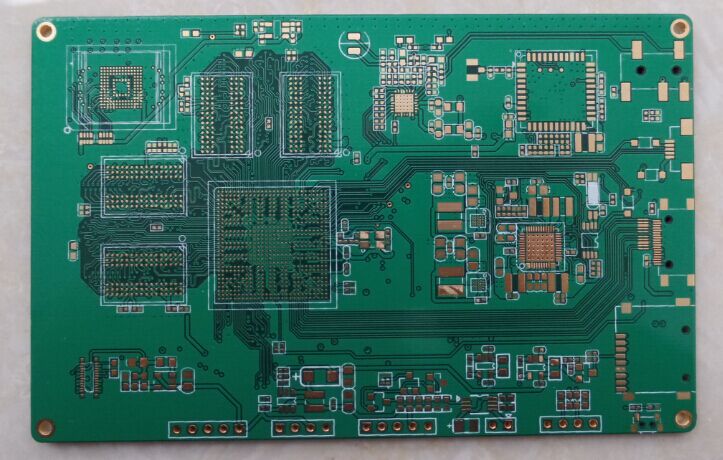
This week,  we finished production for a very difficult HDI PCB with mixed blind vias and buried vias. It took us 15 days to finish samples, because it need many extra lamination process. Our customer is very satisfied with our work and quality.  Upon customer's agreement, here below I share some photos.
8 Layer HDI PCB
Blind vias, L1-L2, L7-L8
Buried vias, L2-L7
BGA work
line width/space: 3mil/3mil
ENIG finishing
Application: Medical, Aerospace, Telecommunications, Robotics, embedded


Baggio WANG FAN
SHENZHEN JAAPSON TECHNOLOGY CO LTD
baggio@jaapson-pcb.com  
www.jaapsonpcb.com
skype: baggiowang0214
JAAPSON, Expert in HDI Multi-layer PCB Manufacturing


Wednesday, July 29, 2015

Ball Grid Array (BGA)-JAAPSON PCB

The capability of minimizing the values of the distinctive parameters of the Ball Grid Array technology (BGA) is a basic requirement to give and adequate answer to the requests for increasing miniaturization, coming from quite all the electronic sectors.

JAAPSON PCB is more than able to respect the most restrictive technical requirements. Being nowadays BGA pitches of 0.5 mm, JAAPSON R&D laboratories already realized a BGA pitch of 0.3 mm, exceeding the actual limits set by SMT (Surface Mounting Technology).


Capabilities
Pitch*
Outer Layer
400 μm
 
Inner Layer
400 μm
Pad**
Outer Layer
300 μm
 
Inner Layer
230 μm
Track
Outer Layer
25 μm
 
Inner Layer
25 μm
Insulation
Outer Layer
25 μm
 
Inner Layer
25 μm
Vias Diameter
Laser
40 μm
 
Mechanical
50 μm
* on customer request Pitch outer and inner layer 200 μm
** on customer request Pad outer and inner layer 200 μm


SHENZHEN JAAPSON TECHNOLOGY CO LTD
Building 2, Tongfuyu Industrial Park,Shenzhen, China, 518104
Tel: 86-755-82596922
Fax:86-755-82596922/82596923
skype: jaapsoncircuits
lisa@jaapson-pcb.com
www.jaapsonpcb.com

JAAPSON, The Expert in HDI Multi-layer PCBs