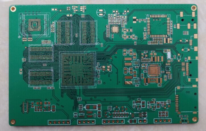
HDI is the abbreviation for High Density Interconnector. HDI PCB is defined as a PCB with a higher wiring density per unit area than conventional PCB. They have finer lines and spaces, smaller vias and capture pads and higher connection pad density than employed in conventional PCB technology.
HDI PCB is used to reduce size and weight, as well as to enhance electrical performance of the
device. HDI PCB is made through Microvia and buried vias and sequential lamination with insulation materials and conductor wiring for higher density of routing. HDI PCB is the best alternative to high layer-countand expensive standard laminate or sequentially laminated boards.
Concerning the electrical requirements for high-speed signal, the PCB must possess some AC characteristics, such as impedance control, high-frequency transmission capability and reduce unnecessary radiation. Multi-layered design is necessary for the structure of Stripline and Microstrip. In order to lesson the quality issues of signal transmission, the insulating material with low dielectric factor and low attenuation ratio is applied. Duo to the miniaturization and arrays of the electronic components, the PCB must be improved in the density. Along with the outcome of the assembling methods of Ball Grid Array, Chip Scale Package and Direct Chip Attachment, the PCB is featured with unprecedented high-density. The hole with a diameter less than 150um is known as Microvia. It can improve the effectiveness of assembly and space utilization and so on. It’s also necessary for the miniaturization of electronic products.
There were a lot of different names for the PCB with such structures. For example, it was called SBU (Sequence Build up the Process) in European and American industry as the program production is in the constructive mode of sequence. It was called MVP (Microvia Process) in Japanese industry because the hole of such products is much smaller than the previous one. It was also called BUM (Build up Multilayer Board) because the traditional multilayer is known as MLB (Multilayer Board).In order to avoid confusion, IPC Printed Circuit Association proposed to call it HDI (High Density Interconnection Technology) as the common name, but it can not reflect the characteristics of the circuit board. So the majority in the PCB industry define such products as HDI PCB.
There are a lot of advantages with HDI PCB, such as small size, high speed and high frequency. It is the main components of personal computers, portable computers, mobile phones and personal digital assistants. At present, except mobile phones, HDI PCB is also widely used in a variety of other consumer products, such as game consoles and MP3, etc. In addition, the applying of HDI PCB in notebook computer is expected trend since 2006 is in the industry.
Baggio WANG FAN
-----------------------------------------------------------
SHENZHEN JAAPSON TECHNOLOGY CO LTD
Building 2, Tongfuyu Industrial Park,Shenzhen, China, 518104
Tel: 86-755-82596922
Fax:86-755-82596922/82596923
skype: baggiowang0214
JAAPSON, The Expert in HDI Multi-layer PCBs